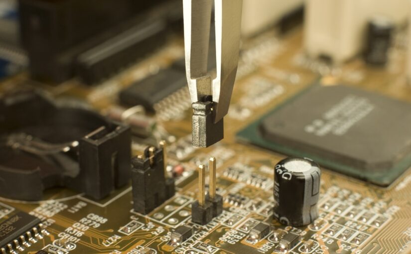
Today, system design relies on high density and high levels of performance – all at a small size. The Very Large Scale Array, or VLSI designs comprising today’s microprocessors are incredibly complex – and incredibly scaled-down.
Advances in design software, such as high-speed PCB design tools, have made these things possible. But as components become ever more tightly packed and miniaturized, and key process parameters ever more numerous, negative forces come into play – such as increased power consumption, enhanced parameter variability, and heat generation – the last being a particular threat.
The increased number of key process parameters in modern CMOS (Complementary metal-oxide semiconductor) VLSI designs causes dramatic on-chip substrate and metal line temperature rises, which impact on reliability, causing timing failure and performance degradation through electromigration and other effects.
It is estimated that up to 50% of all integrated circuit failures are heat-related. Accurate thermal analysis is therefore essential to system hardware design. It is essential to analyze and reduce on-chip temperature variations and identify and eradicate hotspots before a VLSI design enters commercial production.
A lot of research has gone into CPU power consumption and heat dissipation, with the development of high-performance, low power VLSI and FPGA designs. A number of high-speed PCB design tools incorporate thermal analysis software, often with 3D modelling simulations. However, the data can be difficult to interpret, if thermal physics is not your first language.
We at Enventure Technologies are experienced in all matters of CAD design. Our engineering services cover thermal analysis, computational fluid dynamics and many other areas.